- 您现在的位置:买卖IC网 > Sheet目录1999 > ICS9EX21831AKLF (IDT, Integrated Device Technology Inc)IC FANOUT/BUFFER DIFF 72VFQFN
IDT
Eighteen Output Differential Buffer w/2 input mux for PCIe Gen1/2/3
1678D—03/23/12
9EX21831
Eighteen Output Differential Buffer w/2 input mux for PCIe Gen1/2/3
6
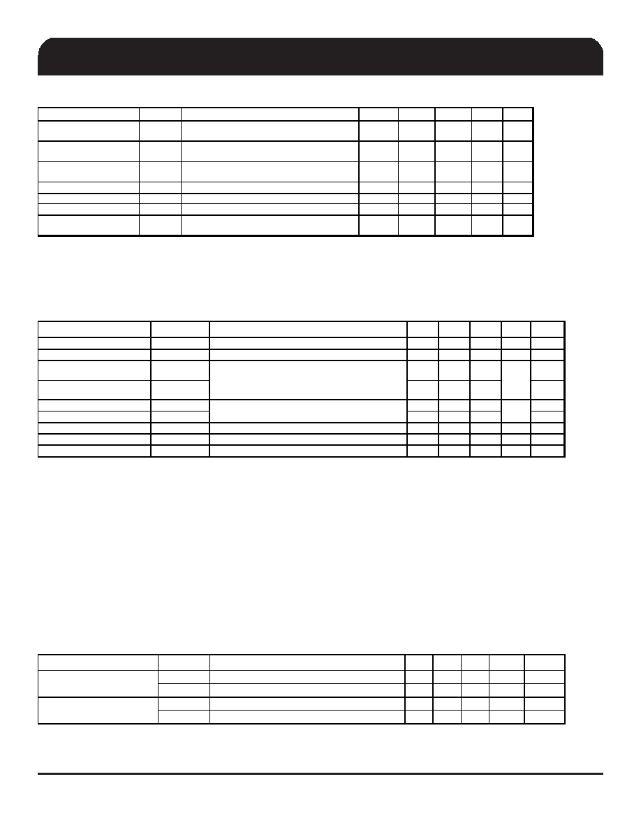
Electrical Characteristics - Clock Input Parameters
TA = TCOM; Supply Voltage VDD/VDDA = 3.3 V +/-5%
PARAMETER
SYMBOL
CONDITIONS
MIN
TYP
MAX
UNITS NOTES
Input High Voltage - DIF_IN
VIHDIF
Differential inputs
(single-ended measurement)
300
750
1150
mV
1
Input Low Voltage - DIF_IN
VILDIF
Differential inputs
(single-ended measurement)
VSS - 300
0
300
mV
1
Input Common Mode
Voltage - DIF_IN
VCOM
Common Mode Input Voltage
150
350
1000
mV
1,3
Input Amplitude - DIF_IN
VSWING
Peak to Peak value
300
mV
1
Input Slew Rate - DIF_IN
dv/dt
Measured differentially
0.4
8
V/ns
1,2
Input Duty Cycle
dtin
Measurement from differential wavefrom
45
55
%
1,4
Input Jitter - Cycle to Cycle
JDIFIn
Differential Measurement
0
125
ps
1
1 Guaranteed by design and characterization, not 100% tested in production.
2Slew rate measured through +/-75mV window centered around differential zero
3Any combination of V
SWING and VCOM is acceptable as long as VSWING >300mV and VIH is <1150mV.
4The device works over a wider range, but the user must take into account duty cycle distortion and required output duty cycle, if using the part in bypass mode.
Electrical Characteristics - DIF 0.7V Current Mode Differential Outputs
TA = TCOM; Supply Voltage VDD/VDDA = 3.3 V +/-5%
PARAMETER
SYMBOL
CONDITIONS
MIN
TYP
MAX
UNITS NOTES
Slew rate
Trf
Scope averaging on
1
2.1
4
V/ns
1, 2, 3
Slew rate matching
DTrf
Slew rate matching, Scope averaging on
12.5
20
%
1, 2, 4
Voltage High
VHigh
660
749
850
1
Voltage Low
VLow
-150
4
150
1
Max VoltageVmax
1150
1
Min Voltage
Vmin
-300
1
Vswing
Scope averaging off
300
mV
1, 2
Crossing Voltage (abs)
Vcross_abs
Scope averaging off
250
333
550
mV
1, 5
Crossing Voltage (var)
D-Vcross
Scope averaging off
140
mV
1, 6
2 Measured from differential waveform
5 Vcross is defined as voltage where Clock = Clock# measured on a component test board and only applies to the differential rising
edge (i.e. Clock rising and Clock# falling).
6 The total variation of all Vcross measurements in any particular system. Note that this is a subset of V_cross_min/max (V_cross
absolute) allowed. The intent is to limit Vcross induced modulation by setting V_cross_delta to be smaller than V_cross absolute.
mV
Statistical measurement on single-ended signal
using oscilloscope math function. (Scope
averaging on)
Measurement on single ended signal using
absolute value. (Scope averaging off)
mV
1Guaranteed by design and characterization, not 100% tested in production. IREF = VDD/(3xR
R).
For RR = 475 (1%), IREF = 2.32mA.
IOH = 6 x IREF and VOH = 0.7V @ ZO=50 (100 differential impedance).
3 Slew rate is measured through the Vswing voltage range centered around differential 0V. This results in a +/-150mV window around
differential 0V.
4 Matching applies to rising edge rate of Clock / falling edge rate of Clock#. It is measured in a +/-75mV window centered on the
average cross point where Clock rising meets Clock# falling. The median cross point is used to calculate the voltage thresholds the
oscilloscope uses for the edge rate calculations.
Electrical Characteristics - Current Consumption
TA = TCOM; Supply Voltage VDD/VDDA = 3.3 V +/-5%
PARAMETER
SYMBOL
CONDITIONS
MIN
TYP
MAX UNITS
NOTES
IDD3.3OP
VDD. All outputs active @100MHz, CL=2pF
340
425
mA
1
IDD3.3AOP
VDDA. All outputs active @100MHz, CL=2pF
30
40
mA
1
IDD3.3PDZ
VDD, All differential pairs tri-stated
12
15
mA
1
IDD3.3APDZ
VDDA, All differential pairs tri-stated
13
20
mA
1
1Guaranteed by design and characterization, not 100% tested in production.
Operating Supply Current
Powerdown Current
发布紧急采购,3分钟左右您将得到回复。
相关PDF资料
ICS9FG1901HKLFT
IC FREQUENCY GENERATOR 72-QFN
ID82C54
IC OSC PROG TIMER 8MHZ 24DIP
IDT2308A-4DCI8
IC CLOCK MULT ZD HI DRV 16-SOIC
IDT2309-1HPGGI
IC CLK BUFFER ZD HI DRV 16-TSSOP
IDT2309A-1HPGG
IC CLK BUFFER ZD HI DRV 16-TSSOP
IDT2309B-1HPGGI
IC CLK BUFFER HIGH DRIVE 16TSSOP
IDT23S05-1HDCGI
IC CLK BUFFER PLL HI DRV 8-SOIC
IDT23S05E-1HDCGI8
IC CLK BUFFER PLL HI DRV 8-SOIC
相关代理商/技术参数
ICS9EX21831AKLFT
功能描述:IC FANOUT/BUFFER DIFF 72VFQFN RoHS:是 类别:集成电路 (IC) >> 时钟/计时 - 专用 系列:PCI Express® (PCIe) 标准包装:1,500 系列:- 类型:时钟缓冲器/驱动器 PLL:是 主要目的:- 输入:- 输出:- 电路数:- 比率 - 输入:输出:- 差分 - 输入:输出:- 频率 - 最大:- 电源电压:3.3V 工作温度:0°C ~ 70°C 安装类型:表面贴装 封装/外壳:28-SSOP(0.209",5.30mm 宽) 供应商设备封装:28-SSOP 包装:带卷 (TR) 其它名称:93786AFT
ICS9FG1001AGLF
功能描述:IC GENERATOR ZD FREQ 56-TSSOP RoHS:是 类别:集成电路 (IC) >> 时钟/计时 - 专用 系列:PCI Express® (PCIe) 标准包装:1,500 系列:- 类型:时钟缓冲器/驱动器 PLL:是 主要目的:- 输入:- 输出:- 电路数:- 比率 - 输入:输出:- 差分 - 输入:输出:- 频率 - 最大:- 电源电压:3.3V 工作温度:0°C ~ 70°C 安装类型:表面贴装 封装/外壳:28-SSOP(0.209",5.30mm 宽) 供应商设备封装:28-SSOP 包装:带卷 (TR) 其它名称:93786AFT
ICS9FG1001AGLFT
功能描述:IC GENERATOR ZD FREQ 56-TSSOP RoHS:是 类别:集成电路 (IC) >> 时钟/计时 - 专用 系列:PCI Express® (PCIe) 标准包装:1,500 系列:- 类型:时钟缓冲器/驱动器 PLL:是 主要目的:- 输入:- 输出:- 电路数:- 比率 - 输入:输出:- 差分 - 输入:输出:- 频率 - 最大:- 电源电压:3.3V 工作温度:0°C ~ 70°C 安装类型:表面贴装 封装/外壳:28-SSOP(0.209",5.30mm 宽) 供应商设备封装:28-SSOP 包装:带卷 (TR) 其它名称:93786AFT
ICS9FG1001BGLF
功能描述:IC GENERATOR ZD FREQ 56TSSOP RoHS:是 类别:集成电路 (IC) >> 时钟/计时 - 专用 系列:* 标准包装:28 系列:- 类型:时钟/频率发生器 PLL:是 主要目的:Intel CPU 服务器 输入:时钟 输出:LVCMOS 电路数:1 比率 - 输入:输出:3:22 差分 - 输入:输出:无/是 频率 - 最大:400MHz 电源电压:3.135 V ~ 3.465 V 工作温度:0°C ~ 85°C 安装类型:表面贴装 封装/外壳:64-TFSOP (0.240",6.10mm 宽) 供应商设备封装:64-TSSOP 包装:管件
ICS9FG1001BGLFT
功能描述:IC GENERATOR ZD FREQ 56TSSOP RoHS:是 类别:集成电路 (IC) >> 时钟/计时 - 专用 系列:* 标准包装:28 系列:- 类型:时钟/频率发生器 PLL:是 主要目的:Intel CPU 服务器 输入:时钟 输出:LVCMOS 电路数:1 比率 - 输入:输出:3:22 差分 - 输入:输出:无/是 频率 - 最大:400MHz 电源电压:3.135 V ~ 3.465 V 工作温度:0°C ~ 85°C 安装类型:表面贴装 封装/外壳:64-TFSOP (0.240",6.10mm 宽) 供应商设备封装:64-TSSOP 包装:管件
ICS9FG104CGLF
功能描述:IC FREQ TIMING GENERATOR 28TSSOP RoHS:是 类别:集成电路 (IC) >> 时钟/计时 - 专用 系列:PCI Express® (PCIe) 标准包装:1 系列:- 类型:时钟/频率发生器,多路复用器 PLL:是 主要目的:存储器,RDRAM 输入:晶体 输出:LVCMOS 电路数:1 比率 - 输入:输出:1:2 差分 - 输入:输出:无/是 频率 - 最大:400MHz 电源电压:3 V ~ 3.6 V 工作温度:0°C ~ 85°C 安装类型:表面贴装 封装/外壳:16-TSSOP(0.173",4.40mm 宽) 供应商设备封装:16-TSSOP 包装:Digi-Reel® 其它名称:296-6719-6
ICS9FG104CGLFT
功能描述:IC FREQ TIMING GENERATOR 28TSSOP RoHS:是 类别:集成电路 (IC) >> 时钟/计时 - 专用 系列:PCI Express® (PCIe) 标准包装:1 系列:- 类型:时钟/频率发生器,多路复用器 PLL:是 主要目的:存储器,RDRAM 输入:晶体 输出:LVCMOS 电路数:1 比率 - 输入:输出:1:2 差分 - 输入:输出:无/是 频率 - 最大:400MHz 电源电压:3 V ~ 3.6 V 工作温度:0°C ~ 85°C 安装类型:表面贴装 封装/外壳:16-TSSOP(0.173",4.40mm 宽) 供应商设备封装:16-TSSOP 包装:Digi-Reel® 其它名称:296-6719-6
ICS9FG104DFILF
功能描述:IC FREQ TIMING GENERATOR 28-SSOP RoHS:是 类别:集成电路 (IC) >> 时钟/计时 - 专用 系列:PCI Express® (PCIe) 标准包装:28 系列:- 类型:时钟/频率发生器 PLL:是 主要目的:Intel CPU 服务器 输入:时钟 输出:LVCMOS 电路数:1 比率 - 输入:输出:3:22 差分 - 输入:输出:无/是 频率 - 最大:400MHz 电源电压:3.135 V ~ 3.465 V 工作温度:0°C ~ 85°C 安装类型:表面贴装 封装/外壳:64-TFSOP (0.240",6.10mm 宽) 供应商设备封装:64-TSSOP 包装:管件